It is an open secret that the hardware in our smart devices contains not only plastics but also conflict minerals such as tungsten, tin, tantalum, silver and gold.
We are exploring different materials, sentient, low-impact, non-toxic, fair traded, recycled and urban mined means of production.
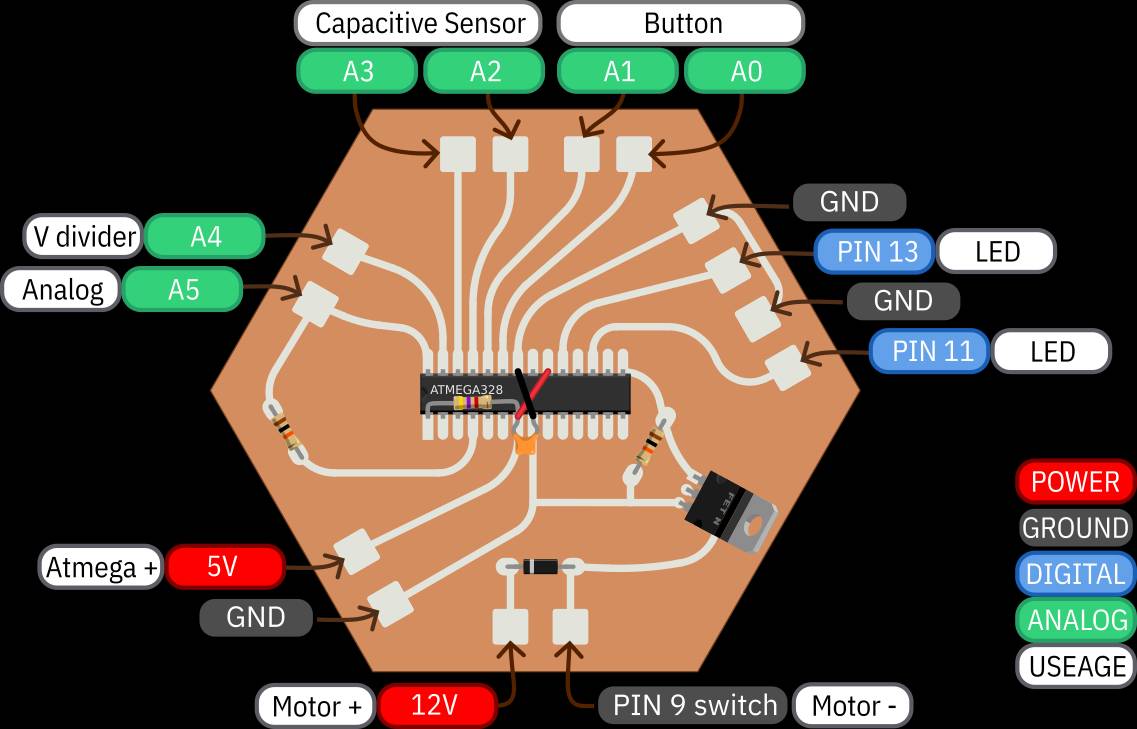
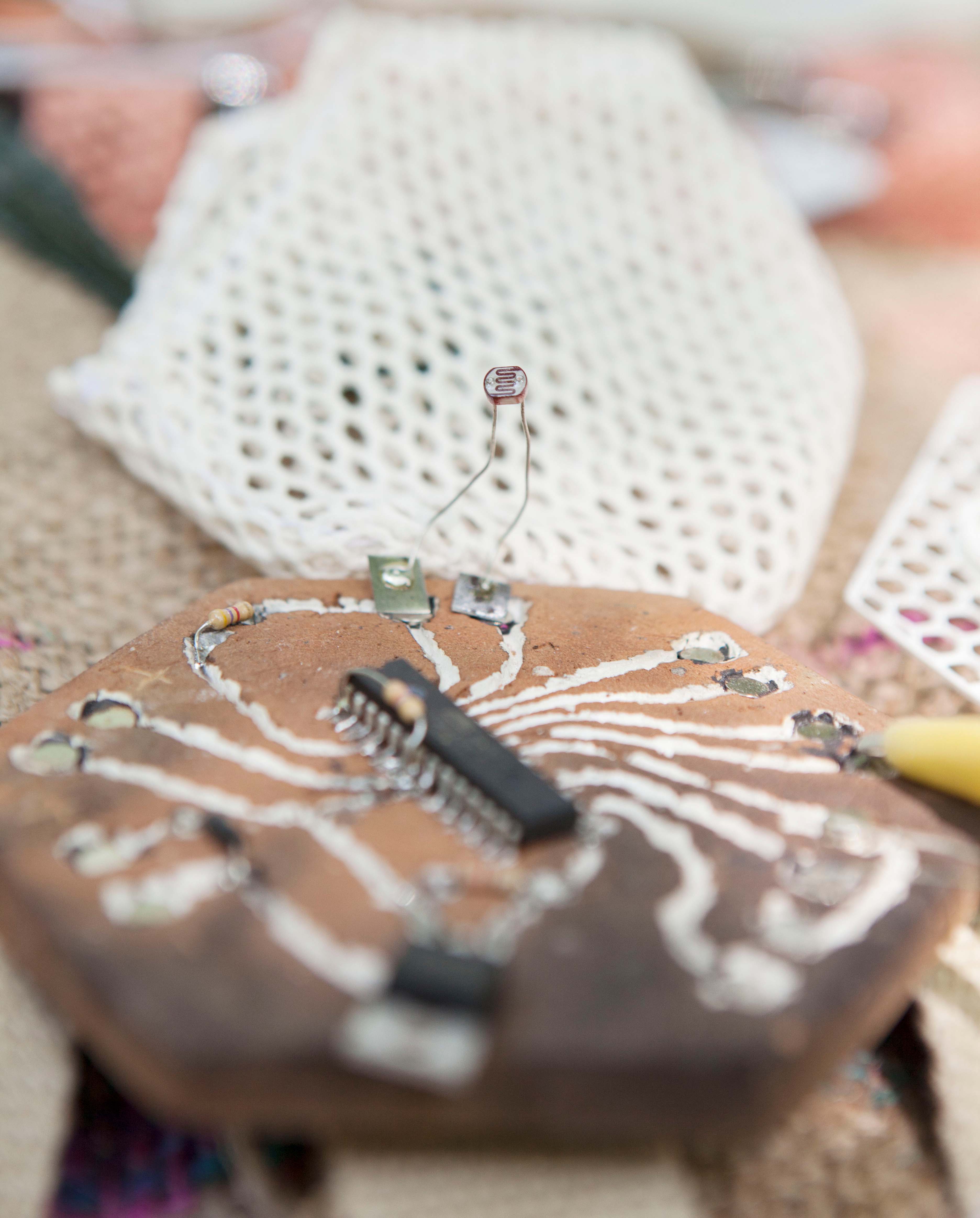
Our initial idea was to develop a microcontroller PCB that could work with the ATmega328P chip, which is commonly used in the famous Arduino Uno board (orArduina board, as some feminists call it). Why this chip? Because we are part of a community hackerspace –
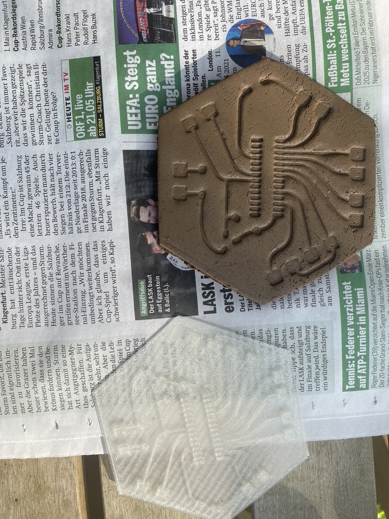
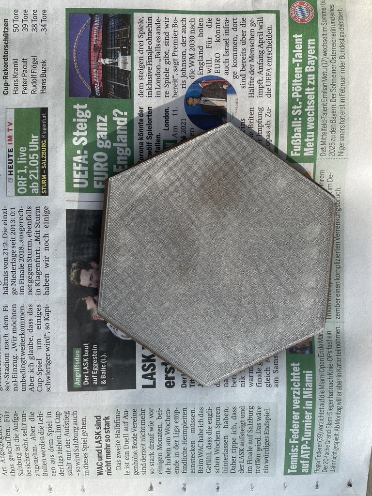
With this insight, we were able to design a 3D printed !stamp‘ using a recycled polypropylene filament. This process took a while, because we had to consider the clay’s changed size after drying and firing. All clay shrinks considerably during the drying and firing process. We estimate that there is a 5% shrinking rate, but this might vary depending on the clay you are working with. We also experimented with the depth of the circuit tracks and realised that the imprint should ideally be 1.2 mm deep.
To build the base of our PCB, we needed insulating, sustainable and robust materials (eggshells? wood plates? wax? ceramics?). We immediately chose ceramics, specificallyporcelain, as it already plays an important role in electronic components such as capacitors, piezo, resistors, and so on. Porcelain is an industrially made material comprising kaolin (the main ingredient that makes it plastic and white) and stone pottery (the second ingredient that makes porcelain translucent and hard). Both are well-known commodities that are prospected and mined around the world, on a small scale in Europe and a larger scale in China, Brazil, South Africa and Vietnam (among others).
It was when we were struggling with the question of how to manufacture clay in low-energy and low-impact ways that we came across the work of Heinz Lackinger, a pottery crafter in Donnerskirchen, Burgenland, Austria, who works with prehistoric techniques of firing clay in an open wood fire. Instead of using sophisticated machines, he uses a simple hole in the grounds of his 18th-century house. We had the privilege of spending two days with this skilled craftsman, learning how to identify and collect the clay, and how to model and fire it using old, dry branches collected from the forest ground. If the clay is collected with awareness of its many qualities, and in small quantities only, this process can be defined as 100% fair trade and congruent with locally sourced modes of hardware production. We owe the knowledge required for the following steps to Heinz Lackinger’s generous knowledge transfer during his workshop, and to our own experiments later applying this technique in the making of natural clay PCB boards.
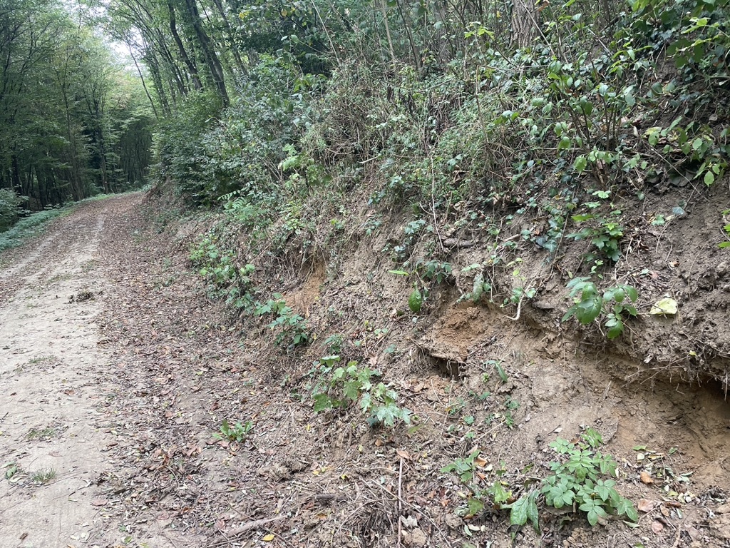
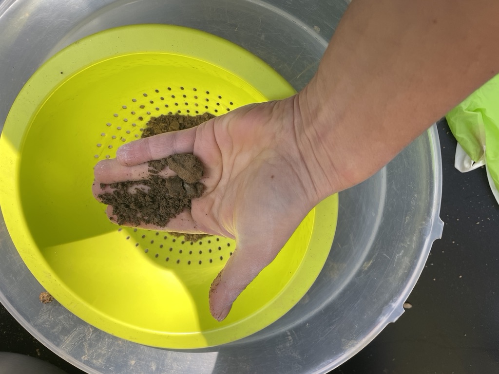
We collected our clay at the beginning of autumn in dry weather. The soil is mainly dry at this time, but it doesn’t consist of argil alone: you will find small stones, plants, even small insects. When the clay is that dry, the easiest way to clean it is using a net that retains the undesirable waste. Our favourite tool for this is a standard kitchen colander. The waste collected should be given back to the earth, put back in the ground.
For the shape of our PCB board, we used a hexagon tile cutter measuring 10 x 10 cm, which can be bought in most ceramic shops. We chose a hexagon shape, as the tile form is not mandatory; but you can pick any shape and thickness you desire, as long as it maintains a printable surface of c. 10 x 10 cm. We chose this shape and format in the hope of assembling the boards as tiles next to one another, connecting them electronically. We ultimately abandoned this idea, since it was very difficult with this material to obtain straight edges that exactly lined up.
You will notice that the clay is very fragile and less elastic than the industrial type. It
tends to split at the edges, which is fine, as long as it is not part of your inner cutter
area.